In 2000, ATI switched to the Radeon branding still in use today. The first member of that family was simply called the Radeon DDR, and it was based on the R100 GPU. The R100 was an evolution of the Rage 128 Pro, but it featured a hardware Transform and Lighting (T&L) engine. It also had two pixel pipelines and three TMUs. ATI added a feature called HyperZ consisting of three technologies: Z compression, Fast Z clear, and a Hierarchical Z-buffer, which combined to conserve memory bandwidth and improve rendering efficiency.
The Radeon DDR also marked ATI's transition to a new 180 nm fabrication process, which helped the company push clock rates as high as 183 MHz on the 64 MB version (a 32 MB card was also available with a 166 MHz GPU).
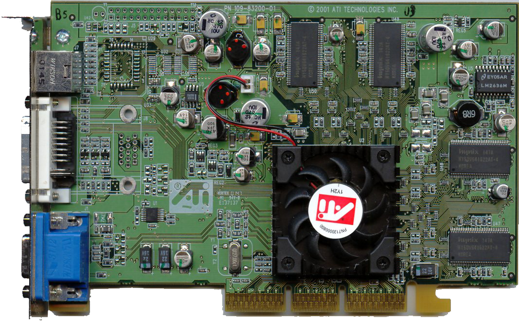
SPECS
Overview
Manufacturer: AMD
Original Series: Radeon
Release Date: June 1st, 2000
PCB Code: 109-70600-00
P/N Code: 102-70601-00
Model: AMD 706 SKU 001
Graphics Processing Unit
GPU Model: R100
Architecture: ATI R100
Fabrication Process: 180 nm
Die Size: 97 mm2
Transistors Count: 30M
Transistors Density: 309.3K TRAN/mm2
Pixel Pipelines: 2
Vertex Pipelines: 1
TMUs: 6
ROPs: 2
Clocks
Base Clock: 183 MHz
Boost Clock: TBD
Memory Clock: 183 MHz
Effective Memory Clock: 366 Mbps
Memory Configuration
Memory Size: 32 MB
Memory Type: DDR
Memory Bus Width: 128-bit
Memory Bandwidth: 5.9 GB/s
Physical
Interface: AGP 4x
Height: 1-slot
Power Connectors: TDP/TBP23 W
Recommended: PSU300 W
Multi-GPU Support: Unsupported
Display Outputs: VGA 1 ×
API Support
DirectX: 7.0
Vulkan: -
OpenGL: 1.3
OpenCL: -
Shader Model: -
Performance
Pixel Fillrate: 366 Pixels/s
Texture Fillrate: 1.1 GTexel/s
SPFP Performance: 732 FLOPS
Performance per W: 32 FLOPS/W
Performance per mm2: 8 FLOPS/mm2
2- ATI All-In-Wonder Radeon 7500 (2001)

In 2001, ATI transitioned to 150 nm manufacturing. The first GPU to benefit from the new node was RV200, used in the All-In-Wonder Radeon 7500 (along with the Radeon 7500 and 7500 LE). Architecturally, RV200 was identical to R100. But it allowed ATI to push core frequency much higher.
The All-in-Wonder board incorporated ATI's Rage Theater chip, along with a TV tuner on-board, giving it serious multimedia chops that Nvidia was never able to counter effectively.
SPECS
Manufacturer: AMD
Original Series: All-in-Wonder
Release Date: August 14th, 2001
PCB Code: 109-83900-00
P/N Code: 102-83905-03
Model: AMD 839 SKU 005
Graphics Processing Unit
GPU Model: RV200
Architecture: ATI R200
Fabrication Process: 150 nm
Die Size: 68 mm2
Transistors Count: 60M
Transistors Density: 882.4K TRAN/mm2
Pixel Pipelines: 1
TMUs: 3
ROPs: 1
Clocks
Base Clock: 290 MHz
Boost Clock: TBD
Memory Clock: 230 MHz
Effective Memory Clock: 460 Mbps
Memory Configuration
Memory Size: 64 MB
Memory Type: DDR
Memory Bus Width: 64-bit
Memory Bandwidth: 3.7 GB/s
Physical
Interface: AGP 4x
Height: 1-slot
Built-in Tuner: Yes
Power Connectors: -
Multi-GPU Support: Unsupported
Display Outputs
DVI-I DualLink: 1 ×
CATV: Yes
API Support
DirectX: 8.1
Vulkan: -
OpenGL: 1.4
OpenCL: -
Shader Model: 1.4
Performance
Pixel Fillrate: 290 Pixels/s
Texture Fillrate: 870 Texel/s
SPFP Performance: 580 FLOPS
Performance per mm2: 9 FLOPS/mm2
3-ATI All-In-Wonder Radeon 8500 (2001)

The All-in-Wonder Radeon 8500 used ATI's R200 GPU with four pixel pipelines and two TMUs per pipe, along with a pair of vertex shaders. Through its implementation, ATI supported Microsoft's Pixel Shader 1.4 spec. The company also rolled out HyperZ II with R200, improving the technology's efficiency.
A core clock rate of 260 MHz and 128 MB of 550 MHz DDR memory landed the All-in-Wonder 8500 close to the performance of AMD's Radeon 8500, which was enough to compete against Nvidia's GeForce 3.
A core clock rate of 260 MHz and 128 MB of 550 MHz DDR memory landed the All-in-Wonder 8500 close to the performance of AMD's Radeon 8500, which was enough to compete against Nvidia's GeForce 3.
SPECS
Overview
Manufacturer: AMD
Original Series: All-in-Wonder
Release Date: November 14th, 2001
PCB Code: 109-83600-00
Board Model: AMD 836
Graphics Processing Unit
GPU Model: R200
Architecture: ATI R200
Fabrication Process: 150 nm
Die Size: 68 mm2
Transistors Count: 60M
Transistors Density: 882.4K TRAN/mm2
Pixel Pipelines: 4
Vertex Pipelines: 2
TMUs: 4
ROPs: 4
Clocks
Base Clock: 230 MHz
Boost Clock: TBD
Memory Clock: 190 MHz
Effective Memory Clock: 380 Mbps
Memory Configuration
Memory Size: 128 MB
Memory Type: DDR
Memory Bus Width: 128-bit
Memory Bandwidth: 6.1 GB/s
Interface: AGP 4x
Height: 1-slot
Built-in Tuner: Yes
Power Connectors: -
TDP/TBP: 23 W
Recommended PSU: 300 W
Display Outputs
DVI-I DualLink: 1 ×
CATV: Yes
API Support
DirectX: 8.1
Vulkan: -
OpenGL: 1.4
OpenCL: -
Shader Model: 1.4
Performance
Pixel Fillrate: 920 Pixels/s
Texture Fillrate: 920 Texel/s
SPFP Performance: 1.8 GFLOPS
Performance per W: 80 FLOPS/W
Performance per mm2: 27 FLOPS/mm2
4- ATI Radeon 9700 Pro (2002)

For the Radeon 9700 Pro, ATI used a completely new architecture. Its R300 GPU employed eight pixel pipelines with one texture unit each, along with four vertex shaders, dramatically increasing geometry processing and textured fillrate. The big 110 million-transistor chip was manufactured using a 150 nm process, just like R200, but it enjoyed higher clock rates thanks to flip-chip packaging.
The design also implemented the Pixel Shader 2.0 specification, and was the first GPU to support Microsoft's DirectX 9 API. To keep the eight-pipe design fed, ATI connected it to 128 MB of DDR memory on a 256-bit interface, yielding just under 20 GB/s of throughput. Third-generation HyperZ helped maximize what ATI could get from the memory subsystem, and derivative cards were able to get away with half as much RAM on a 128-bit bus.
With the Radeon 9700 Pro clocked at 325 MHz, ATI beat Nvidia's flagship GeForce4 Ti 4600 to claim the performance crown. ATI later released a slightly slower version called the Radeon 9700, which was just a lower-clocked Radeon 9700 Pro.
SPECS
Overview
Manufacturer: AMD
Original Series: Radeon 9000
Release Date: July 1st, 2002
PCB Code: 109-94200-11
P/N Code: 102-94206-10
Model: AMD 942 SKU 006
Graphics Processing Unit
GPU Model: R300
Architecture: ATI R300
Fabrication Process: 150 nm
Die Size: 218 mm2
Transistors Count: 110M
Transistors Density: 504.6K TRAN/mm2
Pixel Pipelines: 8
Vertex Pipelines: 4
TMUs: 8
ROPs: 8
Clocks
Base Clock: 325 MHz
Boost Clock: TBD
Memory Clock: 310 MHz
Effective Memory Clock: 620 Mbps
Memory Configuration
Memory Size: 128 MB
Memory Type: DDR
Memory Bus Width: 256-bit
Memory Bandwidth: 19.8 GB/s
Physical
Interface: AGP 8x
Height: 1-slot
Power Connectors: -
Display Outputs
DVI-I DualLink: 1 ×
VGA: 1 ×
S-Video: 1 ×
API Support
DirectX: 9.0
Vulkan: -
OpenGL: 2.0
OpenCL: -
Shader Model: 2.0
Performance
Pixel Fillrate: 2.6 GPixels/s
Texture Fillrate: 2.6 GTexel/s
SPFP Performance: 5.2 GFLOPS
Performance per mm2: 24 FLOPS/mm2
5- ATI Radeon 9800 Pro (2003)

In an attempt to combat the Radeon 9700 Pro, Nvidia launched its GeForce FX 5800 Ultra. This narrowed the performance gap, but was not enough to overtake the Radeon 9700 Pro. To cement its position, ATI introduced a subtle update called the Radeon 9800 Pro that utilized an R350 GPU at higher clock rates. ATI later followed up with a model sporting 256 MB of memory.
The Radeon 9800 Pro extended ATI's performance lead, but would later fall behind when Nvidia released the GeForce FX 5900. Although the Radeon 9800 Pro subsequently gave up its crown, it was still less expensive, more compact, and loaded with other advantages that kept it desirable.
The Radeon 9800 Pro extended ATI's performance lead, but would later fall behind when Nvidia released the GeForce FX 5900. Although the Radeon 9800 Pro subsequently gave up its crown, it was still less expensive, more compact, and loaded with other advantages that kept it desirable.
SPECS
Overview
Manufacturer: AMD
Original Series: Radeon 9000
Release Date: October 1st, 2003
Launch Price: $399 USD
PCB Code: 109-A09400-00
P/N Code: 102-A09401-00
Model: AMD A094 SKU 001
Graphics Processing Unit
GPU Model: R360
Architecture: ATI R300
Fabrication Process: 150 nm
Die Size: 218 mm2
Transistors Count: 117M
Transistors Density: 536.7K TRAN/mm2
Pixel Pipelines: 8
Vertex Pipelines: 4
TMUs: 8
ROPs: 8
Clocks
Base Clock: 380 MHz
Boost Clock: TBD
Memory Clock: 340 MHz
Effective Memory Clock: 680 Mbps
Memory Configuration
Memory Size: 256 MB
Memory Type: DDR
Memory Bus Width: 256-bit
Memory Bandwidth: 21.8 GB/s
Physical
Interface: AGP 8x
Height: 1-slot
Power Connectors: 1 × Molex
TDP/TBP: 47 W
Recommended PSU: 300 W
Display Outputs
DVI-I DualLink: 1 ×
VGA: 1 ×
S-Video: 1 ×
API Support
DirectX: 9.0
Vulkan: -
OpenGL: 2.0
OpenCL: -
Shader Model: 2.0
Performance
Pixel Fillrate: 3 GPixels/s
Texture Fillrate: 3 GTexel/s
SPFP Performance: 6.1 GFLOPS
Performance per W: 129 FLOPS/W
Performance per mm2: 28 FLOPS/mm2
6- ATI Radeon X800 XT (2004)

The rivalry between ATI and Nvidia continued as Nvidia launched its GeForce 6800 GPU and reclaimed its technology and performance lead in the graphics card market. ATI fired back with its X800 XT. The card's R420 GPU had 16 pixel pipelines that were organized into groups of four. Compatibility was limited to Shader Model 2.0b at a time when Nvidia's NV40 had SM 3.0 support. But the GPU also had 16 TMUs, 16 ROPs, and six vertex shaders. R420 connected to 256 MB of GDDR3 over a 256-bit bus and used a new memory compression technique called 3Dc, which helped make the use of available bandwidth more efficient.
Competition between the X800 XT and the GeForce 6800 Ultra was fierce, but in the end, Nvidia held on to its performance crown.
It is also worth noting that the X800 series was the first generation of graphics cards from ATI to feature CrossFire support.
Competition between the X800 XT and the GeForce 6800 Ultra was fierce, but in the end, Nvidia held on to its performance crown.
It is also worth noting that the X800 series was the first generation of graphics cards from ATI to feature CrossFire support.
SPECS
Overview
Manufacturer: AMD
Original Series: Radeon X
Release Date: December 1st, 2004
PCB Code: 109-A31900-00
P/N Code: 102-A31965-00
Model: AMD A319 SKU 065
Graphics Processing Unit
GPU Model: R423
Architecture: ATI R400
Fabrication Process: 130 nm
Die Size: 289 mm2
Transistors Count: 160M
Transistors Density: 553.6K TRAN/mm2
Pixel Pipelines: 16
Vertex Pipelines: 6
TMUs: 16
ROPs: 16
Clocks
Base Clock: 500 MHz
Boost Clock: TBD
Memory Clock: 500 MHz
Effective Memory Clock: 1000 Mbps
Memory Configuration
Memory Size: 256 MB
Memory Type: GDDR3
Memory Bus Width: 256-bit
Memory Bandwidth: 32 GB/s
Physical
Interface: PCI-Express 1.0 x16
Height: 1-slot
Power Connectors: 1 × 6-pin
TDP/TBP: 54 W
Recommended PSU: 350 W
Display Outputs
DVI-I DualLink: 1 ×
VGA: 1 ×
S-Video: 1 ×
API Support
DirectX: 9.0b
Vulkan: -
OpenGL: 2.0
OpenCL: -
Shader Model: 2.0b
Performance
Pixel Fillrate: 8 GPixels/s
Texture Fillrate: 8 GTexel/s
SPFP Performance: 16 GFLOPS
Performance per W: 296 FLOPS/W
Performance per mm2: 55 FLOPS/mm2

8- ATI Radeon X850 XT PE (2004)

Late in 2004, ATI launched a new flagship called the Radeon X850 XT PE. This card used an R480 core built with 130 nm transistors. It was essentially just a die shrink of the R420, but operated at somewhat higher clock rates. This resulted in a modest performance boost, and the X850 XT PE was more competitive against Nvidia's GeForce 6800 Ultra.
SPECS
Overview
Manufacturer: HIS
Original Series: Radeon X
Based On: Radeon X850 XT Platinum
Custom Series: HIS IceQ
Cooling Solution: HIS IceQ2
Released After: December 21st, 2004
Graphics Processing Unit
GPU Model: R480
Architecture: ATI R400
Fabrication Process: 130 nm
Die Size: 297 mm2
Transistors Count: 160M
Transistors Density: 538.7K TRAN/mm2
Pixel Pipelines: 16
Vertex Pipelines: 6
TMUs: 16
ROPs: 16
Clocks
Base Clock: 540 MHz
Boost Clock: TBD
Memory Clock: 590 MHz
Effective Memory Clock: 1180 Mbps
Memory Configuration
Memory Size: 256 MB
Memory Type: GDDR3
Memory Bus Width: 256-bit
Memory Bandwidth: 37.8 GB/s
Physical
Interface: PCI-Express 1.0 x16
Height: 2-slot
Power Connectors: -
TDP/TBP: 67 W
Recommended PSU: 350 W
API Support
DirectX: 9.0b
Vulkan: -
OpenGL: 2.0
OpenCL: -
Shader Model: 2.0b
9- ATI Radeon X1800 XT (2005)

ATI's next graphics core was known as R520, and it was used inside of the original X1000-series flagship. This allowed ATI to support the Shader Model 3.0 specification. The company also shifted to TSMC's 90 nm manufacturing process.
The R520 was designed around an Ultra-Threading Dispatch processor, which broke shader data down into as many as 512 parallel threads that were then executed by a graphics quad pixel shader core. As the name suggested, each quad was made up of four pixel pipelines.
The original X1000-series flagship was the Radeon X1800 XT. It came armed with four quads (16 pixel pipelines), eight vertex shaders, 16 TMUs, and 16 ROPs. The core used a unique memory interface that consisted of two 128-bit buses operating in a ring. Data moved on and off the ring-bus at four different points. This effectively increased memory latency, but reduced memory congestion due to the unique way the dispatch processor handled workloads.
The Radeon X1800 XT shipped with either 256 or 512 MB of GDDR3. Clocked at 625 MHz, the Radeon X1800 XT was highly competitive against Nvidia's GeForce 7800 GTX.
SPECS
Overview
Manufacturer: AMD
Original Series: Radeon X1K
Release Date: October 1st, 2005
Launch Price: $549 USD
PCB Code: 109-A52031-50
P/N Code: 102-A52001-10
Model: AMD A520 SKU 001
Graphics Processing Unit
GPU Model: R520 XT (R520)
Architecture: ATI R500
Fabrication Process: 90 nm
Die Size: 288 mm2
Transistors Count: 321M
Transistors Density: 1.1M TRAN/mm2
Pixel Pipelines: 16
Vertex Pipelines: 8
TMUs: 16
ROPs: 16
Clocks
Base Clock: 600 MHz
Boost Clock: TBD
Memory Clock: 700 MHz
Effective Memory Clock: 1400 Mbps
Memory Configuration
Memory Size: 512 MB
Memory Type: GDDR3
Memory Bus Width: 256-bit
Memory Bandwidth: 44.8 GB/s
Physical
Interface: PCI-Express 1.0 x16
Height: 2-slot
Power Connectors: 1 × 6-pin
TDP/TBP: 113 W
Recommended PSU: 450 W
Display Outputs
DVI-I DualLink: 2 ×
VIVO: 1 ×
API Support
DirectX: 9.0c
Vulkan: -
OpenGL: 2.0
OpenCL: -
Shader Model: 3.0
Performance
Pixel Fillrate: 9.6 GPixels/s
Texture Fillrate: 9.6 GTexel/s
SPFP Performance: 19.2 GFLOPS
Performance per W: 170 FLOPS/W
Performance per mm2: 67 FLOPS/mm2
10- ATI Radeon X1900 XTX (2006)

The following year, ATI launched the R580 GPU, which powered its Radeon X1900 XTX. The key difference between the Radeon X1800 XT and Radeon X1900 XTX was that the Radeon X1900 XTX had three times as many pixel pipelines (48) and quads (12). The rest of the core's resources were unchanged. This had mixed results, as the X1900 XTX could in some cases be nearly three times as fast as the X1800 XT. In other games, however, it could perform nearly identical to the X1800 XT.
SPECS
Overview
Manufacturer: AMD
Original Series: Radeon X1K
Release Date: January 24th, 2006
Launch Price: $399 USD
PCB Code: 109-A52031-50
P/N Code: 180-A52021-50
Model: AMD A520 SKU 021
Graphics Processing Unit
GPU Model: R580
Architecture: ATI R500
Fabrication Process: 90 nm
Die Size: 352 mm2
Transistors Count: 384M
Transistors Density: 1.1M TRAN/mm2
Pixel Pipelines: 48
Vertex Pipelines: 8
TMUs: 16
ROPs: 16
Clocks
Base Clock: 650 MHz
Boost Clock: TBD
Memory Clock: 775 MHz
Effective Memory Clock: 1550 Mbps
Memory Configuration
Memory Size: 512 MB
Memory Type: GDDR3
Memory Bus Width: 256-bit
Memory Bandwidth: 49.6 GB/s
Physical
Interface: PCI-Express 1.0 x16
Length: 24.2 cm
Height: 2-slot
Power Connectors: 1 × 6-pin
TDP/TBP: 135 W
Recommended PSU: 450 W
Display Outputs
DVI-I DualLink: 2 ×
VIVO: 1 ×
API Support
DirectX: 9.0c
Vulkan: -
OpenGL: 2.0
OpenCL: -
Shader Model: 3.0
Performance
Pixel Fillrate: 10.4 GPixels/s
Texture Fillrate: 10.4 GTexel/s
SPFP Performance: 62.4 GFLOPS
Performance per W: 462 FLOPS/W
Performance per mm2: 177 FLOPS/mm2
11- ATI Radeon X1950 XTX (2006)

ATI later shifted the Radeon X1900 XTX design to an 80 nm process. This resulted in the RV580+ core inside of its Radeon X1950 XTX. The core was otherwise unchanged, but managed to achieve higher clock rates. Further, ATI paired it with GDDR4 memory. The combined effect enabled higher performance.
The X1950 XTX was intended to hold the line while ATI finished up with the Radeon HD 2000 series, and it was relatively short-lived.
The X1950 XTX was intended to hold the line while ATI finished up with the Radeon HD 2000 series, and it was relatively short-lived.
SPECS
Overview
Manufacturer: AMD
Original Series: Radeon X1K
Release Date: October 17th, 2006
Launch Price: $449 USD
PCB Code: 109-A91531-00
P/N Code: 102-A91501-00
Model: AMD A915 SKU 001
Graphics Processing Unit
GPU Model: R580+
Architecture: ATI R500
Fabrication Process: 80 nm
Die Size: 352 mm2
Transistors Count: 384M
Transistors Density: 1.1M TRAN/mm2
Pixel Pipelines: 48
Vertex Pipelines: 8
TMUs: 16
ROPs: 16
Clocks
Base Clock: 650 MHz
Boost Clock: TBD
Memory Clock: 1000 MHz
Effective Memory Clock: 2000 Mbps
Memory Configuration
Memory Size: 512 MB
Memory Type: GDDR4
Memory Bus Width: 256-bit
Memory Bandwidth: 64 GB/s
Physical
Interface: PCI-Express 1.0 x16
Length: 23 cm
Height: 2-slot
Power Connectors: 1 × 6-pin
TDP/TBP: 125 W
Recommended PSU: 450 W
Display Outputs
DVI-I DualLink: 2 ×
VIVO: 1 ×
API Support
DirectX: 9.0c
Vulkan: -
OpenGL: 2.0
OpenCL: -
Shader Model: 3.0
Performance
Pixel Fillrate: 10.4 GPixels/s
Texture Fillrate: 10.4 GTexel/s
SPFP Performance: 62.4 GFLOPS
Performance per W: 499 FLOPS/W
Performance per mm2: 177 FLOPS/mm2
12- ATI Radeon HD 2900 XT (2007)

ATI introduced an almost entirely new architecture called TeraScale to power its Radeon HD 2000-series products. This was ATI's first unified shader architecture, and it was also the first design introduced after ATI's merger with AMD. TeraScale was designed to be fully compatible with Pixel Shader 4.0 and Microsoft's DirectX 10.0 API. It first appeared inside of the R600 core, which powered the Radeon HD 2900 XT flagship.
The Radeon HD 2900 XT included similar video acceleration features as AMD's older GPUs. This was done in part to reduce the overall production costs of the chip, but also because the CPUs of the time were fast enough to handle media decoding, albeit at higher power consumption.
Although the new card's architecture differed significantly from AMD's Radeon X1000 series, one key element shared between them was the ultra threaded dispatch processor mentioned on the previous page. However, it was updated to increase performance and efficiency. The R600 GPU was manufactured on an 80 nm process, and it had a total of 320 Stream processors, 16 TMUs, and 16 ROPs. The core continued to use a ring bus, in this case populated by eight 64-bit memory controllers connected to 512 MB of GDDR3 or 1 GB of GDDR4.
The Radeon HD 2900 XT performed well, but it was unable to match Nvidia's flagship GeForce 8800 GTX.
SPECS
Overview
Manufacturer: AMD
Original Series: Radeon HD 2000
Release Date: May 14th, 2007
Launch Price: $399 USD
PCB Code: 109-B00631-00
P/N Code: 102-B00602-00
Model: AMD B006 SKU 002
Graphics Processing Unit
GPU Model: R600 XT (R600)
Architecture: ATI VLIW5
Fabrication Process: 80 nm
Die Size: 420 mm2
Transistors Count: 720M
Transistors Density: 1.7M TRAN/mm2
Stream Cores: 320
Thread Processors: 16
SIMD Engines: 4
TMUs: 16
ROPs: 16
Clocks
Base Clock: 743 MHz
Boost Clock: TBD
Memory Clock: 828 MHz
Effective Memory Clock: 1656 Mbps
Memory Configuration
Memory Size: 512 MB
Memory Type: GDDR4
Memory Bus Width: 512-bit
Memory Bandwidth: 106 GB/s
Physical
Interface: PCI-Express 1.0 x16
Length: 24.1 cm
Height: 2-slot
Power Connectors: 1 × 6-pin, 1 × 8-pin
TDP/TBP: 215 W
Recommended PSU: 600 W
Multi-GPU Support: 4-way
Display Outputs
DVI-I DualLink: 2 ×
S-Video: 1 ×
API Support
DirectX: 10.0
Vulkan: -
OpenGL: 3.3
OpenCL: 1.0
Shader Model: 4.0
Performance
Pixel Fillrate: 11.9 GPixels/s
Texture Fillrate: 11.9 GTexel/s
SPFP Performance: 475.5 GFLOPS
Performance per W: 2.2 GFLOPS/W
Performance per mm2: 1.1 GFLOPS/mm2
13- ATI Radeon HD 3870 (2007)

Later in 2007, ATI introduced its Radeon HD 3870. This successor to the Radeon HD 2900 XT used essentially the exact same design, but transitioned to 55 nm manufacturing. AMD also optimized the memory interface and upgraded to PCIe 2.0. The most notable addition to the 3870's R670 GPU was UVD, ATI's hardware-accelerated video decode engine.
ATI gave the Radeon HD 3870 a higher clock rate, yielding a performance advantage over the previous generation. But it was not significantly faster.
ATI gave the Radeon HD 3870 a higher clock rate, yielding a performance advantage over the previous generation. But it was not significantly faster.
SPECS
Overview
Manufacturer: AMD
Original Series: Radeon HD 3000
Release Date: November 19th, 2007
Launch Price: $269 USD
PCB Code: 109-B33931-00
P/N Code: 102-B33004-00
Model: AMD B339 SKU 004
Graphics Processing Unit
GPU Model: RV670 XT (RV670)
Architecture: ATI VLIW5 TeraScale
Fabrication Process: 55 nm
Die Size: 192 mm2
Transistors Count: 666M
Transistors Density: 3.5M TRAN/mm2
Stream Cores: 320
Thread Processors: 16
SIMD Engines: 4
TMUs: 16
ROPs: 16
Clocks
Base Clock: 777 MHz
Boost Clock: TBD
Memory Clock: 1126 MHz
Effective Memory Clock: 2252 Mbps
Memory Configuration
Memory Size: 512 MB
Memory Type: GDDR4
Memory Bus Width: 256-bit
Memory Bandwidth: 72.1 GB/s
Physical
Interface: PCI-Express 2.0 x16
Length: 24.1 cm
Height: 2-slot
Power Connectors: 1 × 6-pin
TDP/TBP: 106 W
Recommended PSU: 450 W
Multi-GPU Support: 4-way
Display Outputs
DVI-I DualLink: 2 ×
S-Video: 1 ×
API Support
DirectX: 10.1
Vulkan: -
OpenGL: 3.3
OpenCL: 1.2
Shader Model: 4.1
Performance
Pixel Fillrate: 12.4 GPixels/s
Texture Fillrate: 12.4 GTexel/s
SPFP Performance: 497.3 GFLOPS
Performance per W: 4.7 GFLOPS/W
Performance per mm2: 2.6 GFLOPS/mm2
14- ATI Radeon HD 4870 (2008)

As ATI's Radeon HD 2900 XT and Radeon HD 3870 were unable to compete with Nvidia's latest, the company desperately needed a new high-end GPU. This came in 2008 in the form of the RV770, inside of its Radeon HD 4870 utilizing the same architecture as its predecessor on a 55 nm process. The core had 800 Stream processors, 40 TMUs, and 16 ROPs connected to either 512 MB or 1 GB of memory on a 256-bit bus. Since GDDR5 was relatively new at the time, it only operated at 900 MHz. Still, this gave the Radeon HD 4870 an abundance of memory bandwidth.
The GPU was clocked roughly the same as the Radeon HD 3870 at 750 MHz, but due to the added execution resources and steep increase in memory bandwidth, the Radeon HD 4870 was quite a bit faster. It couldn't catch Nvidia's GeForce GTX 280, but was significantly less expensive and highly competitive for its time. It also marked ATI's return to the high-end GPU market.
The GPU was clocked roughly the same as the Radeon HD 3870 at 750 MHz, but due to the added execution resources and steep increase in memory bandwidth, the Radeon HD 4870 was quite a bit faster. It couldn't catch Nvidia's GeForce GTX 280, but was significantly less expensive and highly competitive for its time. It also marked ATI's return to the high-end GPU market.
SPECS
Overview
Manufacturer: AMD
Original Series: Radeon HD 4000
Release Date: June 25th, 2008
Launch Price: $299 USD
PCB Code: 109-B50731-10
P/N Code: 102-B50701-10
Model: AMD B507 SKU 001
Graphics Processing Unit
GPU Model: RV770 PRO (RV770)
Architecture: ATI VLIW5 TeraScale
Fabrication Process: 55 nm
Die Size: 256 mm2
Transistors Count: 956M
Transistors Density: 3.7M TRAN/mm2
Stream Cores: 800
Thread Processors: 40
SIMD Engines: 10
TMUs: 40
ROPs: 16
Clocks
Boost Clock: TBD
Memory Clock: 900 MHz
Effective Memory Clock: 1800 Mbps
Memory Configuration
Memory Size: 512 MB
Memory Type: GDDR3
Memory Bus Width: 256-bit
Memory Bandwidth: 57.6 GB/s
Physical
Interface: PCI-Express 2.0 x16
Length: 25 cm
Height: 2-slot
Power Connectors: 2 × 6-pin
TDP/TBP: 150 W
Recommended PSU: 450 W
Multi-GPU Support: 3-way
Display Outputs
DVI-I DualLink: 2 ×
S-Video: 1 ×
API Support
DirectX: 10.1
Vulkan: -
OpenGL: 3.3
OpenCL: 1.2
Shader Model: 4.1
Performance
Pixel Fillrate: 12 GPixels/s
Texture Fillrate: 30 GTexel/s
SPFP Performance: 1.2 TFLOPS
Performance per W: 8 GFLOPS/W
Performance per mm2: 4.7 GFLOPS/mm2
14- ATI Radeon HD 4890 (2009)

ATI went through the RV770 die and tweaked it to facilitate higher clock rates, resulting in the Radeon HD 4890's RV790 GPU. This card was clocked 100 MHz faster than the Radeon HD 4870, but was otherwise identical. Performance increased, if only slightly.
SPECS
Overview
Manufacturer: AMD
Original Series: Radeon HD 4000
Release Date: April 2nd, 2009
Launch Price: $249 USD
PCB Code: 109-B79031-00
P/N Code: 102-B79002-00
Model: AMD B790 SKU 002
Graphics Processing Unit
GPU Model: RV790 XT (RV790)
Architecture: ATI VLIW5 TeraScale
Fabrication Process: 55 nm
Die Size: 282 mm2
Transistors Count: 959M
Transistors Density: 3.4M TRAN/mm2
Stream Cores: 800
Thread Processors: 40
SIMD Engines: 10
TMUs: 40
ROPs: 16
Clocks
Base Clock: 850 MHz
Boost Clock: TBD
Memory Clock: 975 MHz
Effective Memory Clock: 3900 Mbps
Memory Configuration
Memory Size: 1024 MB
Memory Type: GDDR5
Memory Bus Width: 256-bit
Memory Bandwidth: 124.8 GB/s
Physical
Interface: PCI-Express 2.0 x16
Length: 24.1 cm
Height: 2-slot
Power Connectors: 2 × 6-pin
TDP/TBP: 190 W
Recommended PSU: 500 W
Multi-GPU Support: 3-way
Display Outputs
DVI-I DualLink: 2 ×
S-Video: 1 ×
API Support
DirectX: 10.1
Vulkan: -
OpenGL: 3.3
OpenCL: 1.2
Shader Model: 4.1
Performance
Pixel Fillrate: 13.6 GPixels/s
Texture Fillrate: 34 GTexel/s
SPFP Performance: 1.4 TFLOPS
Performance per W: 7.2 GFLOPS/W
Performance per mm2: 4.8 GFLOPS/mm2
15- ATI Radeon HD 5870 (2009)

The Radeon HD 4890 didn't sit on top of ATI's product line-up for long, as the company launched its Radeon HD 5870 later the same year. It used a new TeraScale II architecture designed to support DirectX 11. A key improvement moving from TeraScale to TeraScale II was that the individual Stream processors were capable of handling a wider array of instructions.
The Cypress core inside of Radeon HD 5870 had 1600 Stream processors, 80 TMUs, and 32 ROPs. The Radeon HD 5870 operated at 850 MHz, and it connected to 1 GB of GDDR5 over a 256-bit interface. The core was etched using 40 nm transistors, which helped reduce power consumption despite the more complex GPU. Overall, the Radeon HD 5870 was nearly twice as fast as its predecessor, and for a time it claimed the performance crown as the fastest GPU in the world.
The Cypress core inside of Radeon HD 5870 had 1600 Stream processors, 80 TMUs, and 32 ROPs. The Radeon HD 5870 operated at 850 MHz, and it connected to 1 GB of GDDR5 over a 256-bit interface. The core was etched using 40 nm transistors, which helped reduce power consumption despite the more complex GPU. Overall, the Radeon HD 5870 was nearly twice as fast as its predecessor, and for a time it claimed the performance crown as the fastest GPU in the world.
SPECS
Overview
Manufacturer: AMD
Original Series: Radeon HD 5000
Release Date: September 23rd, 2009
Launch Price: $399 USD
PCB Code: 109-C00137-00
P/N Code: 102-C00103-20
Model: AMD C001 SKU 003
Graphics Processing Unit
GPU Model: Cypress XT (Cypress)
Architecture: VLIW5 TeraScale 2
Fabrication Process: 40 nm
Die Size: 334 mm2
Transistors Count: 2.2B
Transistors Density: 6.4M TRAN/mm2
Stream Cores: 1600
Thread Processors: 80
SIMD Engines: 20
TMUs: 80
ROPs: 32
Clocks
Base Clock: 850 MHz
Boost Clock: TBD
Memory Clock: 1200 MHz
Effective Memory Clock: 4800 Mbps
Memory Configuration
Memory Size: 1024 MB
Memory Type: GDDR5
Memory Bus Width: 256-bit
Memory Bandwidth: 153.6 GB/s
Physical
Interface: PCI-Express 2.0 x16
Width: 11.2 cm
Length: 28.2 cm
Height: 2-slot
Power Connectors: 2 × 6-pin
TDP/TBP: 188 W
Recommended PSU: 500 W
Multi-GPU Support: 4-way
Display Outputs
DVI-D DualLink: 2 ×
DisplayPort: 1 ×
HDMI: 1 ×
API Support
DirectX: 11.0
Vulkan: -
OpenGL: 4.4
OpenCL: 1.2
Shader Model: 5.0
Performance
Pixel Fillrate: 27.2 GPixels/s
Texture Fillrate: 68 GTexel/s
SPFP Performance: 2.7 TFLOPS
Performance per W: 14.5 GFLOPS/W
Performance per mm2: 8.1 GFLOPS/mm2
16- AMD Radeon HD 6970 (2010)

AMD acquired ATI back in 2006, but continued to use ATI's brand until the introduction of the Radeon HD 6000 series.
The company realized that the Cypress GPU was incapable of keeping the Stream processors adequately fed. This was inefficient, as all of the cores were powered, but some were idle. The solution was to reduce the number of Stream processors slightly, which resulted in an increase in efficiency and GPU utilization. AMD then added new SIMD engines, though the end result was a 6000-series with fewer resources than its predecessor. This architecture became known as TeraScale 3.
The 6000-series flagship, AMD's Radeon HD 6970, shipped with 1536 Stream processors, 96 TMUs, and 32 ROPs. The 6970's Cypress GPU was manufactured using 40 nm transistors. It also used the same 256-bit bus, but had access to 2 GB of GDDR5. The architectural improvements allowed the 6970 to outperform AMD's previous effort while also being more energy efficient overall.
The 6000-series flagship, AMD's Radeon HD 6970, shipped with 1536 Stream processors, 96 TMUs, and 32 ROPs. The 6970's Cypress GPU was manufactured using 40 nm transistors. It also used the same 256-bit bus, but had access to 2 GB of GDDR5. The architectural improvements allowed the 6970 to outperform AMD's previous effort while also being more energy efficient overall.
SPECS
Overview
Manufacturer: AMD
Original Series: Radeon HD 6000
Release Date: December 14th, 2010
Launch Price: $369 USD
PCB Code: 109-C20047-00
P/N Code: 102-C20001-01
Model: AMD C200 SKU 001
Graphics Processing Unit
GPU Model: Cayman XT (Cayman)
Architecture: VLIW4 TeraScale 2
Fabrication Process: 40 nm
Die Size: 389 mm2
Transistors Count: 2.6B
Transistors Density: 6.8M TRAN/mm2
Stream Cores: 1536
Thread Processors: 96
SIMD Engines: 24
TMUs: 96
ROPs: 32
Clocks
Base Clock: 880 MHz
Boost Clock: TBD
Memory Clock: 1375 MHz
Effective Memory Clock: 5500 Mbps
Memory Configuration
Memory Size: 2048 MB
Memory Type: GDDR5
Memory Bus Width: 256-bit
Memory Bandwidth: 176 GB/s
Physical
Interface: PCI-Express 2.0 x16
Width: 11.2 cm
Length: 26.7 cm
Height: 2-slot
Power Connectors: 1 × 6-pin, 1 × 8-pin
TDP/TBP: 250 W
Recommended PSU: 600 W
Multi-GPU Support: 4-way
Display Outputs
DVI-D DualLink: 2 ×
miniDisplayPort: 2 ×
HDMI: 1 ×
API Support
DirectX: 11.0
Vulkan: -
OpenGL: 4.4
OpenCL: 1.2
Shader Model: 5.0
Performance
Pixel Fillrate: 28.2 GPixels/s
Texture Fillrate: 84.5 GTexel/s
SPFP Performance: 2.7 TFLOPS
Performance per W: 10.8 GFLOPS/W
Performance per mm2: 7 GFLOPS/mm2
17- AMD Radeon HD 7970 (2011)

In 2011, AMD left its TeraScale architecture behind in favor of Graphics Core Next, completely re-designed and based on a RISC microarchitecture. One of the company's goals was a processor well-suited for gaming and GPGPU work. As a result, the Radeon HD 7970 saw a sharper increase in compute performance than almost any other discipline. GCN first appeared inside of AMD's Radeon HD 7000-series graphics cards. The flagship Radeon HD 7970 sported 2048 Stream processors, 128 TMUs, and 32 ROPs built with 28 nm transistors. Even with the increase in resources, the Radeon HD 7970's Tahiti GPU was more compact and able to attain higher clock rates than its predecessor. The Radeon HD 7970 launched at 925 MHz, with access to 3 GB of GDDR5 on a 384-bit bus.
The Radeon HD 7970 outperformed all other single-GPU graphics cards by a wide margin. In some games, it was able to beat dual-GPU cards like the Radeon HD 6990 and GeForce GTX 590 as well. It consumed more power than its predecessor, though.
The Radeon HD 7970 outperformed all other single-GPU graphics cards by a wide margin. In some games, it was able to beat dual-GPU cards like the Radeon HD 6990 and GeForce GTX 590 as well. It consumed more power than its predecessor, though.
SPECS
Overview
Manufacturer: AMD
Original Series: Radeon HD 7000
Release Date: December 22nd, 2011
Launch Price: $549 USD
PCB Code: 109-C38611-00
P/N Code: 102-C38601-00
Model: AMD C386 SKU 001
Graphics Processing Unit
GPU Model: Tahiti XT (Tahiti)
Architecture: Graphics Core Next 1.0
Fabrication Process: 28 nm
Die Size: 352 mm2
Transistors Count: 4.3B
Transistors Density: 12.3M TRAN/mm2
Stream Processors: 2048
Compute Units: 128
Shader Engines: 32
TMUs: 128
ROPs: 32
Clocks
Base Clock: 925 MHz
Boost Clock: TBD
Memory Clock: 1375 MHz
Effective Memory Clock: 5500 Mbps
Memory Configuration
Memory Size: 3072 MB
Memory Type: GDDR5
Memory Bus Width: 384-bit
Memory Bandwidth: 264 GB/s
Physical
Interface: PCI-Express 3.0 x16
Width: 11.12 cm
Length: 26.49 cm
Height: 2-slot
Power Connectors: 1 × 6-pin, 1 × 8-pin
Power Design: 5+1+1
TDP/TBP: 230 W
Multi-GPU Support: 4-way
Display Outputs
DVI-D DualLink: 1 ×
miniDisplayPort: 2 ×
HDMI: 1 ×
API Support
DirectX: 11.2
Vulkan: -
OpenGL: 4.4
OpenCL: 1.2
Shader Model: 5.0
Performance
Pixel Fillrate: 29.6 GPixels/s
Texture Fillrate: 118.4 GTexel/s
SPFP Performance: 3.8 TFLOPS
Performance per W: 16.5 GFLOPS/W
Performance per mm2: 10.8 GFLOPS/mm2
18- AMD Radeon HD 8990 (2013)
The Radeon HD 8990 OEM is a high-end graphics card by AMD, launched in April 2013. Built on the 28 nm process, and based on the Malta graphics processor, the card supports DirectX 12.0. The Malta graphics processor is a large chip with a die area of 365 mm² and 4,313 million transistors. Radeon HD 8990 OEM combines two graphics processors to increase performance. It features 2048 shading units, 128 texture mapping units and 32 ROPs per GPU. AMD has placed 6,144 MB GDDR5 memory on the card, which are connected using a 384-bit memory interface per GPU (each GPU manages 3,072 MB). The GPU is operating at a frequency of 950 MHz, which can be boosted up to 1000 MHz, memory is running at 1500 MHz.
SPECS
Overview
Manufacturer: AMD
Based on: HD 7990
Original Series: Radeon HD 8000
Release Date: April 24th, 2013
Launch Price: OEM
PCB Code: 109-C47637-00
Board Model: AMD C476
Graphics Processing Unit
GPU Codename: Malta
GPU Model: 2× Tahiti XT2
Architecture: Graphics Core Next 1.0
Fabrication Process: 28 nm
Die Size: 2× 352 mm2
Transistors Count: 2× 4.3B
Transistors Density: 12.3M TRAN/mm2
Stream Processors: 2× 2048 (4096)
Compute Units: 2× 128 (256)
Shader Engines: 2× 32 (64)
TMUs: 2× 128 (256)
ROPs: 2× 32 (64)
Clocks
Base Clock: 950 MHz
Boost Clock: 1000 MHz
Memory Clock: 1500 MHz
Effective Memory Clock: 6000 Mbps
Memory Configuration
Memory Size: 2× 3072 (6144) MB
Memory Type: GDDR5
Memory Bus Width: 2× 384 (768)-bit
Memory Bandwidth: 2× 288 (576) GB/s
Physical
Interface: PCI-Express 3.0 x16
Width: 13.7 cm
Length: 31.2 cm
Height: 2-slot
Power Connectors: 2 × 8-pin
TDP/TBP: 375 W
Recommended PSU: 750 W
Multi-GPU Support: 4-way
Display Outputs
DVI-D DualLink: 1 ×
miniDisplayPort: 4 ×
API Support
DirectX: 11.2
Vulkan: -
OpenGL: 4.4
OpenCL: 1.2
Shader Model: 5.0
Performance
Pixel Fillrate: 60.8 GPixels/s
Texture Fillrate: 243.2 GTexel/s
SPFP Performance: 7.8 TFLOPS
Performance per W: 20.8 GFLOPS/W
Performance per mm2: 11.1 GFLOPS/mm2
19- AMD Radeon R9 290X (2013)

AMD's Radeon HD 7970 GHz Edition was one of the company's longest-standing flagships. Eventually, it was replaced by the Radeon R9 290X and its Hawaii GPU, which was manufactured using the same 28 nm lithography and based on an updated version of GCN. The size of the L2 cache increased from 768 KB to 1 MB, and AMD improved bandwidth between on-die resources. AMD also introduced its TrueAudio technology, leveraging DSP cores to accelerate audio processing in optimized software.
The Hawaii GPU contained 2816 Stream processors, 176 TMUs, and 64 ROPs connected to 4GB of GDDR5 over a 512-bit bus. The R9 290X was undeniably fast, often outperforming Nvidia's GeForce GTX Titan and GeForce GTX 780. The reference card wasn't perfect, however, as it had serious heat issues that imposed lower clock rates in order to run within its thermal specifications. You could manually set the fan speed higher, though this made the stock thermal solution loud and bothersome. This issue largely vanished after AMD's board partners produced versions of the R9 290X with more efficient coolers, however, and the R9 290X was able to hold the performance crown for awhile.
The Hawaii GPU contained 2816 Stream processors, 176 TMUs, and 64 ROPs connected to 4GB of GDDR5 over a 512-bit bus. The R9 290X was undeniably fast, often outperforming Nvidia's GeForce GTX Titan and GeForce GTX 780. The reference card wasn't perfect, however, as it had serious heat issues that imposed lower clock rates in order to run within its thermal specifications. You could manually set the fan speed higher, though this made the stock thermal solution loud and bothersome. This issue largely vanished after AMD's board partners produced versions of the R9 290X with more efficient coolers, however, and the R9 290X was able to hold the performance crown for awhile.
SPECS
Overview
Manufacturer: AMD
Original Series: Radeon 200
Release Date: October 24th, 2013
Launch Price: $549 USD
PCB Code: 109-C67157-00
P/N Code: 102-C67101-00
Model: AMD C671 SKU 001
Graphics Processing Unit
GPU Model: Hawaii XT (Hawaii)
Architecture: Graphics Core Next 2.0
Fabrication Process: 28 nm
Die Size: 438 mm2
Transistors Count: 6.3B
Transistors Density: 14.4M TRAN/mm2
Stream Processors: 2816
Compute Units: 44
Shader Engines: 4
TMUs: 176
ROPs: 64
Clocks
Base Clock: 1000 MHz
Boost Clock: TBD
Memory Clock: 1250 MHz
Effective Memory Clock: 5000 Mbps
Memory Configuration
Memory Size: 4096 MB
Memory Type: GDDR5
Memory Bus Width: 512-bit
Memory Bandwidth: 320 GB/s
Physical
Interface: PCI-Express 3.0 x16
Power Connectors: 1 × 6-pin, 1 × 8-pin
Power Design: 6+2
TDP/TBP: 300 W
Recommended PSU: 600 W
Multi-GPU Support: 4-way
Display Outputs
DVI-D DualLink: 2 ×
DisplayPort: 1 ×
HDMI: 1 ×
API Support
DirectX: 11.2
Vulkan: 1.0
OpenGL: 4.4
OpenCL: 1.2
Shader Model: 5.0
Performance
Pixel Fillrate: 64 GPixels/s
Texture Fillrate: 176 GTexel/s
SPFP Performance: 5.6 TFLOPS
Performance per W: 18.8 GFLOPS/W
Performance per mm2: 12.9 GFLOPS/mm2
20- AMD Radeon R9 Fury X (2015)

AMD's next flagship also used an updated implementation of the GCN architecture. Its Radeon R9 Fury X sported a Fiji GPU with 8.9 billion transistors, enabling 4096 Stream processors, 256 TMUs, and 64 ROPs. More notable than the massive core, however, was AMD's pioneering introduction of High-Bandwidth Memory. Fiji is fed by 4GB of HBM capable of 512 GB/s over a 4096-bit bus.
Stuck at 28 nm manufacturing and faced with a big, hot GPU, AMD went with liquid cooling to make the Fury X smaller and quieter than would otherwise be possible. The Radeon R9 Fury X outperformed Nvidia's GeForce GTX 980, but traded blows with its GeForce GTX 980 Ti. As a result, determining last generation's king often came down to game selection and quality settings.
Stuck at 28 nm manufacturing and faced with a big, hot GPU, AMD went with liquid cooling to make the Fury X smaller and quieter than would otherwise be possible. The Radeon R9 Fury X outperformed Nvidia's GeForce GTX 980, but traded blows with its GeForce GTX 980 Ti. As a result, determining last generation's king often came down to game selection and quality settings.
SPECS
Overview
Manufacturer: AMD
Original Series: Radeon 300
Release Date: June 24th, 2015
Launch Price: $649 USD
PCB Code: 109-C88057-00
P/N Code: 102-C88001-00
Model: AMD C880 SKU 001
Graphics Processing Unit
GPU Model: Fiji XT (Fiji)
Architecture: Graphics Core Next 3.0
Fabrication Process: 28 nm
Die Size: 596 mm2
Transistors Count: 8.9B
Transistors Density: 14.9M TRAN/mm2
Stream Processors: 4096
Compute Units: 64
Shader Engines: 4
TMUs: 256
ROPs: 64
Clocks
Base Clock: 1000 MHz
Boost Clock: 1050 MHz
Memory Clock: 500 MHz
Effective Memory Clock: 1000 Mbps
Memory Configuration
Memory Size: 4096 MB
Memory Type: HBM
Memory Bus Width: 4096-bit
Memory Bandwidth: 512 GB/s
Physical
Interface: PCI-Express 3.0 x16
Height: 2-slot
Power Connectors: 2 × 8-pin
TDP/TBP: 275 W
Recommended PSU: 600 W
Multi-GPU Support: 4-way
Display Outputs
DisplayPort: 3 ×
HDMI: 1 ×
API Support
DirectX: 11.2
Vulkan: 1.0
OpenGL: 4.4
OpenCL: 2.0
Shader Model: 5.0
Performance
Pixel Fillrate: 64 GPixels/s
Texture Fillrate: 256 GTexel/s
SPFP Performance: 8.2 TFLOPS
Performance per W: 29.8 GFLOPS/W
Performance per mm2: 13.7 GFLOPS/mm2
21- AMD Radeon RX 480 (2016)

AMD's Radeon RX 480 is somewhat unique in that it was not designed to be the company's fastest graphics card. Instead, it was built to be an efficient mid-range board. You can expect higher-end solutions based on the same Polaris architecture in the months to come.
The Radeon RX 480 has 2304 Stream processors, 144 TMUs, and 32 ROPs connected to either 4 or 8GB of GDDR5 on a 256-bit bus. The core operates at a base clock rate of 1120 MHz and can accelerate up to 1266 MHz. The GPU also boasts a large 2MB L2 cache to reduce its dependency on the GDDR5. Officially, the RX 480 is rated for a 150 W TDP. And although it isn't as fast as Nvidia's Pascal-based cards, it does fare well against the GeForce GTX 970.
The Radeon RX 480 has 2304 Stream processors, 144 TMUs, and 32 ROPs connected to either 4 or 8GB of GDDR5 on a 256-bit bus. The core operates at a base clock rate of 1120 MHz and can accelerate up to 1266 MHz. The GPU also boasts a large 2MB L2 cache to reduce its dependency on the GDDR5. Officially, the RX 480 is rated for a 150 W TDP. And although it isn't as fast as Nvidia's Pascal-based cards, it does fare well against the GeForce GTX 970.
AMD also produced lower end RX 470 and RX 460 models to handle the budget market. These GPUs use the same architecture as the RX 480, but with fewer cores and reduced memory support.
SPECS
Overview
Manufacturer: AMD
Original Series: Radeon 400
Release Date: June 29th, 2016
Launch Price: $229 USD
PCB Code: 109-D00947-00A
Device: ID67DF:C7
Board Model: AMD D009
Graphics Processing Unit
GPU Model: Ellesmere XT (Polaris 10)
Architecture: Polaris GCN 4.0
Fabrication Process: 14 nm FinFET
Die Size: 232 mm2
Transistors Count: 5.7B
Transistors Density: 24.6M TRAN/mm2
Stream Processors: 2304
Compute Units: 36
TMUs: 144
ROPs: 32
Clocks
Base Clock: 1120 MHz
Boost Clock: 1266 MHz
Memory Clock: 2000 MHz
Effective Memory Clock: 8000 Mbps
Memory Configuration
Memory Size: 8192 MB
Memory Type: GDDR5
Memory Bus Width: 256-bit
Memory Bandwidth: 256 GB/s
Physical
Interface: PCI-Express 3.0 x16
Width: 12.7 cm
Length: 25.4 cm
Height: 2-slot
Power Connectors: 1 × 6-pin
TDP/TBP: 150 W
Recommended PSU: 450 W
Multi-GPU Support: 4-way
Display Outputs
DisplayPort: 3 ×
HDMI 2.0: 1 ×
API Support
DirectX: 12.0
Vulkan: 1.0
OpenGL: 4.5
OpenCL: 2.1
Shader Model: 5.0
Performance
Pixel Fillrate: 35.8 GPixels/s
Texture Fillrate: 161.3 GTexel/s
SPFP Performance: 5.2 TFLOPS
Performance per W: 34.4 GFLOPS/W
Performance per mm2: 22.2 GFLOPS/mm2

23- AMD Radeon Vega RX 64 (2017)

AMD designed Vega as a high-performance GPU architecture to run concurrently with Polaris. While the pixel shaders used in Vega and Polaris are relatively similar to each other, Vega has the clear advantage thanks to a significant increase in the number of shaders, plus faster memory. AMD implemented HBM2 memory with Vega, and has announced consumer GPUs with 8GB of GBM2 with a peak bandwidth of 484 GB/s over a 4096-bit bus. The workstation oriented Vega Frontier Edition pushes this up to 16GB of HBM2. AMD also reworked the cache inside Vega to increase bandwidth throughout the core. The render back-end is now a client of the L2 cache, which has increased to 4MB.
Vega also has access to a wide number of new features and processing elements. There is a new programmable geometry pipeline that can render 17 primitives per clock. Vega sports a Next-Generation Compute Unit (NCU), equipped with 64 shaders, which is designed to accelerate game performance.
Vega 64 will compete with Nvidia's GeForce GTX 1080, while a lower-end variant called Vega 56 will do battle with the GTX 1070.
SPECS
Overview
Manufacturer: AMD
Original Series: Radeon 500
Release Date: August 14th, 2017
Launch Price: $599 USD
Graphics Processing Unit
GPU Model: Vega 10 XT (Vega 10)
Architecture: Vega GCN 5.0
Fabrication Process: 14 nm FinFET
Die Size: 486 mm2
Transistors Count: 12.5B
Transistors Density: 25.7M TRAN/mm2
Stream Processors: 4096
Compute Units: 64
TMUs: 256
Clocks
Base Clock: 1247 MHz
Boost Clock: 1546 MHz
Memory Clock: 945 MHz
Effective Memory Clock: 1890 Mbps
Memory Configuration
Memory Size: 8192 MB
Memory Type: HBM2
Memory Bus Width: 2048-bit
Memory Bandwidth: 483.8 GB/s
Physical
Interface: PCI-Express 3.0 x16
Height: 2-slot
Power Connectors: 2 × 8-pin
TDP/TBP: 295 W
Recommended PSU: 600 W
Display Outputs
HDMI 2.0: 1 ×
API Support
DirectX: 12.0
Vulkan: 1.0
OpenGL: 4.5
OpenCL: 2.0
Shader Model: 5.0
Performance
Pixel Fillrate: 79.8 GPixels/s
Texture Fillrate: 319.2 GTexel/s
SPFP Performance: 10.2 TFLOPS
Performance per W: 34.6 GFLOPS/W
Performance per mm2: 21 GFLOPS/mm2